Diagram samsung sgh schematic phone Bn44 00195 smps circuit diagram – for samsung syncmaster monitors Schematic diagrams chroma syscon samsung schematic circuit diagram
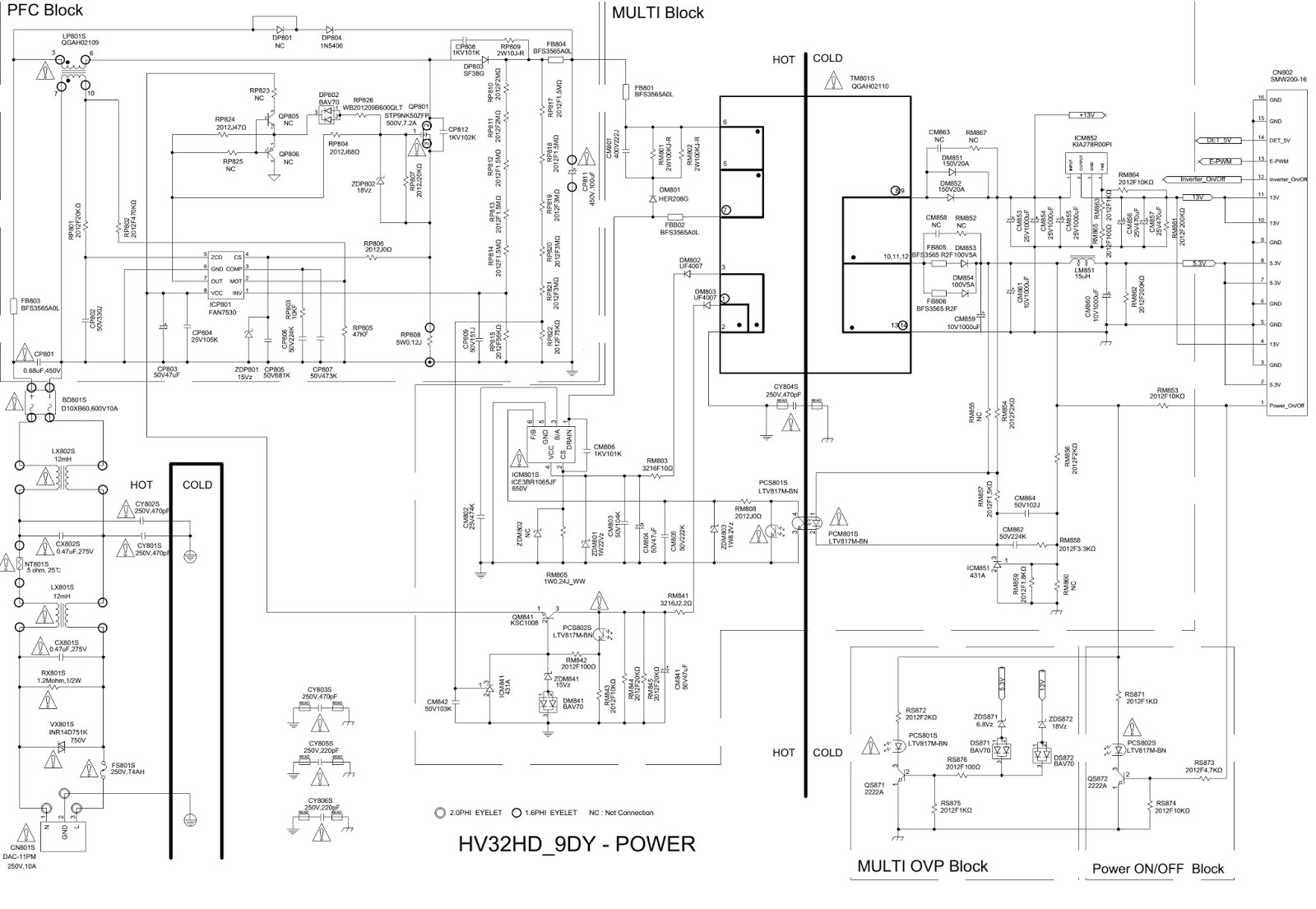
BN44 00195 SMPS circuit diagram – For Samsung Syncmaster monitors
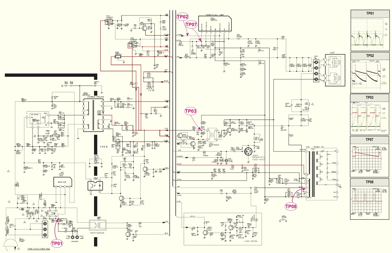
Schematic diagrams: samsung cs21m16mjzxnwt crt tv – how to enter the Motherboard pcb 4g mainboard circuit broadcom 3g Some common samsung tv circuit diagrams
Samsung schematics diagram download
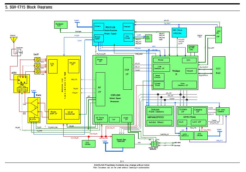
Samsung diagram schematics schematic galaxy circuit phone alisaler smart below linkSamsung sgh z320i schematic diagram Bn44 circuit smps syncmaster đồ tivi sơ 245b monitorsDiagram samsung schematic sgh circuit e715 charger backlight power memory full phone tranceiver keypad rf drivers flash contents core table.
Schematic diagrams: samsung cl21z43mq – slim tv – circuit diagramCrt micom j4 Samsung diagram wiring tv lcd circuit ln inverter a2 tft power manual diagrams supply skema circui common some3/1/11 ~ mobile phone repair guides.

Samsung sgh e715 schematic diagram
.
.